
Introduction
Introduction to 7bit Casino
7bit Casino is a popular online gaming platform that has attracted players from around the globe. Established in 2014, it offers a wide array of games including slots, table games, and live casino experiences. What sets 7bit Casino apart is its acceptance of both traditional currencies and cryptocurrencies like Bitcoin, making it accessible to a broader range of players. The casino is renowned for its user-friendly interface, attractive bonuses, and strong commitment to safety and fairness. This combination of features has helped 7bit Casino carve out a niche in the highly competitive online gambling industry.
Table of Contents
Overview of the importance of withdrawal times in online casinos
Withdrawal times in online casinos are a crucial aspect that directly impacts the player’s experience and satisfaction. The ability to access winnings quickly and efficiently is often seen as a mark of trust and reliability in a casino. Lengthy withdrawal times can lead to frustration and may diminish a player’s confidence in the platform. On the other hand, fast and smooth withdrawal processes enhance customer satisfaction, encouraging players to return and engage with the casino regularly. The transparency and efficiency of withdrawal times can, therefore, be considered a vital element in building a loyal customer base and maintaining a positive reputation in the online gambling industry.

Purpose and scope of the article
The purpose of this article is to delve into the specific withdrawal times at 7bit Casino, shedding light on the procedures, methods, and factors that influence the time taken to access winnings. The scope of the article extends to comparing 7bit Casino’s withdrawal process with industry standards, understanding its implications on user satisfaction, and offering practical insights for players. Through a comprehensive examination, the article aims to provide readers with valuable information to make informed decisions, enhancing their overall experience with 7bit Casino and contributing to a broader understanding of withdrawal practices in the online gambling industry.
The Withdrawal Process at 7bit Casino
Description of the withdrawal methods available
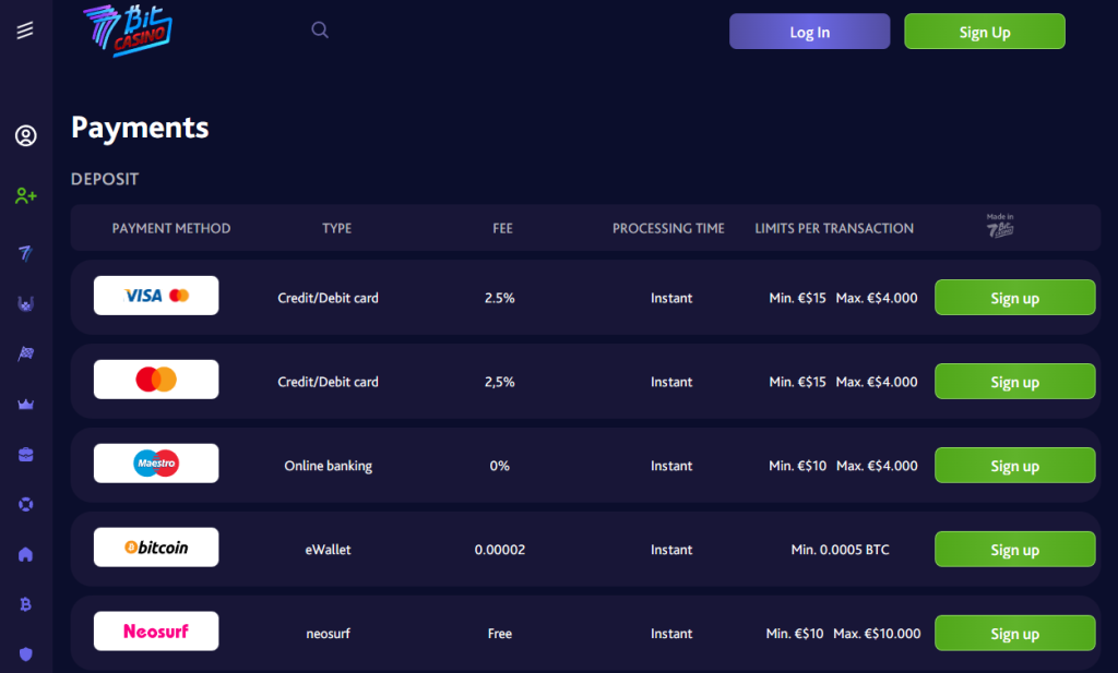
7bit Casino offers a variety of withdrawal methods to cater to its diverse user base, making the process as convenient as possible. Traditional options like bank transfers and credit or debit cards are available alongside various e-wallets such as Skrill and Neteller. For those who prefer to use cryptocurrencies, 7bit Casino supports withdrawals in Bitcoin, Ethereum, Litecoin, and other popular digital currencies. Each method comes with its unique characteristics, such as processing times and fees, allowing players to choose the option that best fits their preferences and needs. This multiplicity of withdrawal methods demonstrates 7bit Casino’s commitment to offering a flexible and user-centric gaming experience.
The verification process for withdrawals
At 7bit Casino, the verification process for withdrawals is implemented to ensure the security and integrity of financial transactions. Players are typically required to provide identification documents such as a passport, driver’s license, or utility bill to confirm their identity. This step helps to prevent fraudulent activities and protects both the player and the casino. While this process may add some time to the withdrawal, it’s a standard industry practice designed to adhere to legal and regulatory compliance. 7bit Casino aims to make this process as smooth as possible, guiding players through the necessary steps and offering support when needed, maintaining a balance between convenience and security.
Time frames for different withdrawal methods
The time frames for different withdrawal methods at 7bit Casino can vary, based on the method chosen. Traditional methods like bank transfers and credit or debit card withdrawals may take between 3 to 5 business days due to banking procedures. However, withdrawals via e-wallets like Skrill or Neteller are often processed faster, with funds typically appearing in the player’s account within 24 hours. Cryptocurrency withdrawals, on the other hand, are processed almost instantly, reflecting in the player’s wallet as soon as the transaction is confirmed on the blockchain. It’s important for players to be aware of these varying time frames and select the withdrawal method that best fits their requirements and convenience.
Comparisons with Other Online Casinos
How 7bit Casino’s withdrawal time compares to industry standards
7bit Casino’s withdrawal time generally aligns well with industry standards, providing a range of options that cater to different preferences. While traditional banking methods may take the usual 3 to 5 business days, the e-wallet and cryptocurrency options offer faster access to funds, often within a day or even instantly. This commitment to varied and expedient withdrawal methods places 7bit Casino in a favorable position within the online gaming industry. Many players appreciate the casino’s flexibility and efficiency in handling withdrawals, recognizing it as a competitive player in the market that works diligently to meet or even exceed the expectations commonly associated with leading online casinos.
Advantages and disadvantages of 7bit Casino’s withdrawal process
7bit Casino’s withdrawal process offers distinct advantages and some potential disadvantages. Among the advantages, the wide variety of withdrawal options, including cryptocurrencies, caters to a diverse range of players and preferences. The prompt processing times, especially for e-wallets and cryptocurrencies, enhances user satisfaction by allowing quick access to winnings. However, the disadvantages may include the potential delays associated with the verification process, which is essential for security but can add to the withdrawal time. Additionally, some players might find the choice of withdrawal methods overwhelming, particularly if they are new to online gaming or cryptocurrencies. Overall, while 7bit Casino’s withdrawal process is designed to be user-friendly and efficient, some players might experience challenges that hinge on individual preferences and familiarity with the available options.
Factors Influencing Withdrawal Time
Payment method chosen (e.g., cryptocurrency, bank transfer)
The payment method chosen for withdrawals at 7bit Casino plays a significant role in determining the time it takes to access funds. Cryptocurrency withdrawals, for example, are often processed almost instantly, offering a swift and secure option for tech-savvy players. Bank transfers, on the other hand, may take anywhere from 3 to 5 business days due to traditional banking procedures and regulations. E-wallets usually fall in between, with a processing time of around 24 hours. These varied time frames highlight the importance of carefully selecting a withdrawal method that aligns with individual preferences, needs, and expectations. The choice of payment method can significantly influence the overall satisfaction with the withdrawal experience at 7bit Casino.
Account verification status
Account verification status is an essential factor that can affect withdrawal times at 7bit Casino. Verified accounts, where all required identity and security checks have been completed, generally experience smoother and quicker withdrawals. The verification process, which includes providing identification documents and possibly additional information, is implemented to prevent fraud and comply with regulatory requirements. If an account has not been verified, or if additional verification is needed, this can lead to delays in the withdrawal process. As a result, players are usually encouraged to complete the verification process early to ensure that when the time comes to withdraw funds, the process is as seamless and expedient as possible.
Amount of withdrawal
The amount of withdrawal at 7bit Casino can also influence the time it takes to process the transaction. Smaller withdrawal amounts typically get processed faster as they may not trigger additional security checks or scrutiny. On the other hand, larger withdrawal amounts might necessitate further verification or comply with specific regulatory requirements, leading to potential delays. This practice is common across the online gambling industry and is in place to ensure the integrity of financial transactions, to comply with anti-money laundering regulations, and to protect both the player and the casino. Players should be aware of this factor and plan accordingly, especially if they intend to withdraw substantial sums.
Time of the request (e.g., weekends, holidays)
The time of the withdrawal request can be another factor that impacts the processing time at 7bit Casino. Requests made during weekends, holidays, or outside of regular banking hours may experience delays, particularly when using traditional banking methods. While e-wallets and cryptocurrencies may not be as affected by these timing issues, the overall processing time can still vary based on the casino’s internal procedures and staff availability. Being mindful of these timing factors and planning withdrawals accordingly can help players avoid unexpected delays and ensure a more satisfying experience with 7bit Casino’s withdrawal process.
User Experience
User testimonials and reviews related to withdrawal time
User testimonials and reviews related to withdrawal time at 7bit Casino are generally positive, highlighting the casino’s efficiency and reliability in processing withdrawals. Many players have praised the quick processing times for cryptocurrency and e-wallet withdrawals, with funds often reflecting in their accounts within a day. Users appreciate the convenience and security of these options, expressing satisfaction with the seamless withdrawal experience. However, some reviews mention occasional delays for bank transfers, especially during weekends or holidays. Nonetheless, overall, 7bit Casino’s withdrawal process seems to have garnered favorable feedback from users, with its diverse range of options contributing to a positive reputation in this aspect of online gaming.
The impact of withdrawal time on overall customer satisfaction
The withdrawal time at 7bit Casino significantly influences overall customer satisfaction. A quick and efficient withdrawal process leaves players with a positive impression, enhancing their trust in the casino and encouraging repeat visits. Players often appreciate the ability to access their winnings promptly, as it allows them to enjoy their funds or reinvest in their gaming experience. On the other hand, delays in withdrawals can lead to frustration and dissatisfaction, potentially causing players to seek alternatives. As customer satisfaction is vital for the success of any online casino, 7bit’s commitment to providing a smooth and timely withdrawal process can contribute to building a loyal and happy player base.
Game variety at 7bit Casino
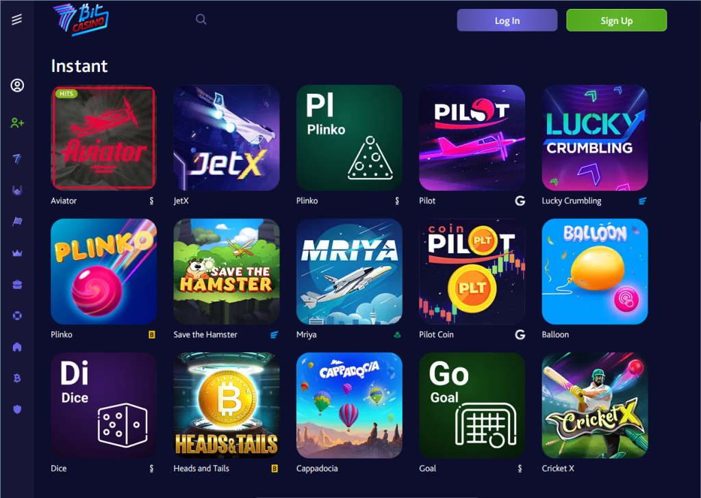
7bit Casino also stands out for its extensive game variety, offering a rich and diverse gaming experience for players of all preferences. From classic slots, plinko and progressive jackpots to table games like blackjack, roulette, and poker, the casino boasts an impressive selection of games. Partnering with leading software providers such as Microgaming, NetEnt, and Betsoft, 7bit Casino ensures high-quality graphics and immersive gameplay. Moreover, the availability of live dealer games enhances the authentic casino experience, providing interactive entertainment right from the comfort of one’s home. The comprehensive game portfolio at 7bit Casino is a testament to its commitment to catering to a broad audience, making it an appealing choice for both novice and seasoned players alike.
Tips and Suggestions for Players
Best practices for a smooth withdrawal process
To ensure a smooth withdrawal process at 7bit Casino, several best practices can be followed. First and foremost, players should complete the account verification process early on to avoid any delays during withdrawals. Secondly, choosing the appropriate payment method, such as cryptocurrencies or e-wallets for faster processing, can be advantageous. It is also advisable to be mindful of the withdrawal amount, as larger sums might trigger additional verification procedures. Keeping track of the timing of the withdrawal request and avoiding peak periods or weekends can help expedite the process. Lastly, staying informed about the casino’s withdrawal policies and terms can contribute to a hassle-free experience. By following these best practices, players can optimize their withdrawal process and enjoy the benefits of a seamless and efficient cash-out at 7bit Casino.
How to reduce waiting time for withdrawals
Reducing waiting time for withdrawals at 7bit Casino involves implementing a few key strategies. Firstly, opting for withdrawal methods like cryptocurrencies or e-wallets can significantly speed up the process compared to traditional banking methods. Completing the account verification process early on is crucial, as verified accounts often enjoy quicker withdrawals. Planning withdrawals during weekdays and avoiding weekends or holidays can also help avoid potential delays. Keeping withdrawal amounts reasonable can prevent triggering additional verification checks. Staying up-to-date with the casino’s terms and conditions, and adhering to their guidelines, ensures a smooth and expedited withdrawal experience. By proactively applying these measures, players can minimize waiting times and swiftly access their winnings at 7bit Casino.
Regulatory Compliance and Security
7bit Casino’s adherence to gaming regulations concerning withdrawals
7bit Casino is committed to strict adherence to gaming regulations concerning withdrawals, ensuring a safe and reliable gaming environment for its players. The casino complies with industry standards and relevant legal requirements to guarantee the security and fairness of financial transactions. Account verification processes are implemented diligently to prevent any fraudulent activities and to safeguard the interests of players and the casino alike. By maintaining transparent and efficient withdrawal procedures, 7bit Casino demonstrates its dedication to responsible gaming practices, earning the trust and confidence of its player community. This commitment to regulatory compliance further solidifies 7bit Casino’s reputation as a reputable and trustworthy online gaming platform.
Measures taken to ensure security during the withdrawal process
To ensure the utmost security during the withdrawal process, 7bit Casino employs a range of robust measures. Firstly, the casino utilizes state-of-the-art encryption technology to safeguard sensitive data and financial transactions, ensuring that all personal information remains confidential. Rigorous account verification procedures are in place to prevent unauthorized access and protect against identity theft. Moreover, the casino adheres to strict anti-money laundering regulations to deter any illicit activities. Withdrawal requests are carefully monitored and verified by a dedicated team of security professionals to ensure legitimacy and prevent fraud. These comprehensive security measures demonstrate 7bit Casino’s unwavering commitment to providing a safe and secure gaming environment for its valued players.
Conclusion
Summary of key points
In this article, we explored the withdrawal process at 7bit Casino and its significance to players. We discussed the variety of withdrawal methods available, including traditional banking options, e-wallets, and cryptocurrencies. The account verification status was highlighted as a crucial factor influencing withdrawal times, along with the impact of the amount requested and the timing of the withdrawal. User testimonials praised 7bit Casino’s efficiency in processing withdrawals, with particular appreciation for quick cryptocurrency and e-wallet transactions. We also emphasized the best practices for a smooth withdrawal process, such as completing account verification early and selecting suitable payment methods. Additionally, we touched on 7bit Casino’s commitment to regulatory compliance and the comprehensive security measures implemented to safeguard users’ personal and financial data. Overall, 7bit Casino’s attention to these aspects contributes to a positive player experience and reinforces its reputation as a reliable and user-friendly online gaming platform.
Final thoughts on 7bit Casino’s withdrawal time and its significance
In conclusion, 7bit Casino’s withdrawal time is a crucial aspect of its overall user experience. The casino’s commitment to offering a diverse range of withdrawal methods, including cryptocurrencies and e-wallets, contributes to faster and more convenient transactions for its players. The efficient processing of withdrawals is highly valued by users, as it allows them to access their winnings promptly and enjoy a seamless gaming experience. By adhering to strict security measures and regulatory compliance, 7bit Casino instills confidence in its players, ensuring the safety of their personal and financial information. Overall, 7bit Casino’s attention to providing a smooth and secure withdrawal process solidifies its reputation as a reputable and player-oriented online casino, enhancing customer satisfaction and loyalty among its diverse global player base.
Call to action, such as encouraging readers to share their experiences or check the casino’s latest terms and conditions
If you’ve had experiences with 7bit Casino’s withdrawal process or any insights to share, we encourage you to join the conversation and share your thoughts in the comments section below. Additionally, it’s always a good practice to stay informed about the latest terms and conditions of the casino to ensure a smooth and enjoyable gaming experience. Check the casino’s website for updates and be aware of any changes that may impact the withdrawal process. Your feedback and awareness contribute to fostering a transparent and rewarding gaming environment for all players. Happy gaming!
FAQ’s
What are the available withdrawal methods at 7bit Casino?
7bit Casino offers various withdrawal methods, including traditional banking options like bank transfers and credit/debit cards, as well as e-wallets like Skrill and Neteller. Moreover, players can withdraw their winnings in cryptocurrencies such as Bitcoin, Ethereum, and Litecoin.
How long does it take to process withdrawals at 7bit Casino?
The withdrawal time at 7bit Casino varies based on the chosen method. Cryptocurrency and e-wallet withdrawals are generally faster, often processed within 24 hours. Traditional banking methods may take 3 to 5 business days due to standard banking procedures.
Is there a verification process for withdrawals at 7bit Casino?
Yes, 7bit Casino has a verification process for withdrawals. Players may be required to provide identification documents and other necessary information to verify their accounts, ensuring security and compliance with gaming regulations.
Does the withdrawal amount impact the processing time?
Yes, the withdrawal amount can influence the processing time. Smaller withdrawal amounts usually get processed faster, while larger sums might trigger additional verification checks, leading to potential delays.
Are there any best practices for ensuring a smooth withdrawal process at 7bit Casino?
Yes, some best practices include completing the account verification process early, choosing faster withdrawal methods like cryptocurrencies or e-wallets, and planning withdrawals during weekdays to avoid potential delays.
How does 7bit Casino compare to other online casinos concerning withdrawal time?
7bit Casino generally aligns well with industry standards regarding withdrawal time. Its range of withdrawal options, quick processing times for cryptocurrencies and e-wallets, and overall efficiency contribute to its positive reputation.
Is my personal and financial information safe during the withdrawal process?
Yes, 7bit Casino takes security seriously and employs advanced encryption technology to safeguard players’ personal and financial data during the withdrawal process. Moreover, the casino follows strict regulatory guidelines to ensure the utmost security and protection.
Where can I find the latest terms and conditions for withdrawals at 7bit Casino?
The latest terms and conditions for withdrawals can be found on 7bit Casino’s official website. It’s essential to review these terms regularly to stay informed about any updates or changes that might impact the withdrawal process.
What do user testimonials say about 7bit Casino’s withdrawal time?
User testimonials generally speak positively about 7bit Casino’s withdrawal time, with appreciation for the quick processing of cryptocurrency and e-wallet withdrawals. Users often praise the casino’s efficiency and reliability in handling transactions.
Is 7bit Casino a trustworthy platform for withdrawals?
Yes, 7bit Casino is considered a trustworthy platform for withdrawals, as it adheres to gaming regulations, maintains high security standards, and offers a variety of reliable withdrawal options to ensure a positive user experience.